


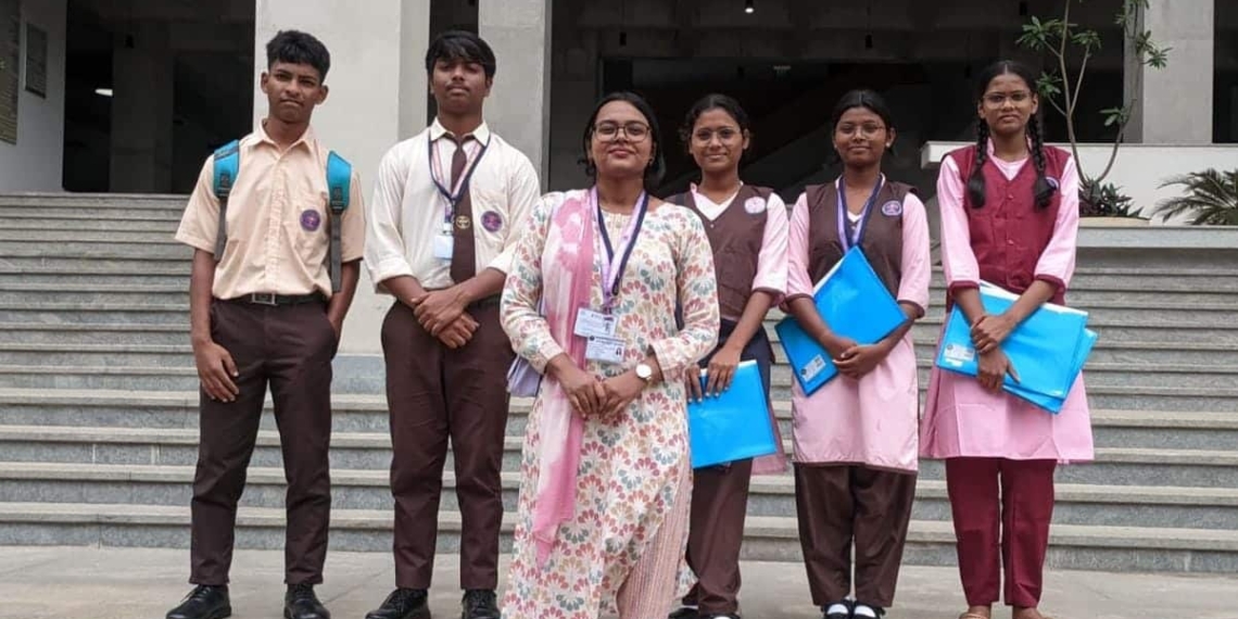
In a significant step towards empowering tribal students with advanced scientific exposure, five Class X students from Odisha’s Eklavya Model Residential Schools (EMRS) participated in a two‑day Semiconductor Training Programme at the Centre for Nano Science and Engineering (CeNSE), IISc Bengaluru.Organised under the STEM Initiative of the Ministry of Tribal Affairs, the programme aimed to provide meritorious students with first‑hand experience in semiconductor science, clean‑room technology, and emerging career opportunities.
The participants included Prabin Kumar Naik and Geetanjali Mahanta (EMRS Gidhibas), Dusmanta Majhi (EMRS Bahalda), Hiramani Baskey and Fulamani Singh (EMRS Dhanghera), accompanied by escort teacher Debasmita Priyadarshini Behera.On the first day, students received orientation on semiconductor basics, clean‑room safety, contamination control, and wafer processing, followed by visits to specialised labs including Optics, Electrical, Mechanical, TEM and SEM facilities.Day two focused on semiconductor fabrication and manufacturing processes, with students introduced to precision techniques, safety protocols, and the strategic importance of semiconductors in India’s technological growth.A career guidance session encouraged students to pursue higher education and explore opportunities in science, engineering, and research. Certificates were distributed at the conclusion of the programme.Officials noted that the exposure to IISc’s advanced research environment is expected to broaden the students’ scientific outlook and motivate them to explore fields such as nanotechnology, electronics, and semiconductor research.This initiative marks a milestone in bridging tribal education with cutting‑edge science, creating pathways for future innovators from Odisha’s EMRS institutions.